Our end-to-end nanodevice foundry process
Our Nanodevice Foundry covers the fabrication process from initial carbon nanotube growth to final device testing. We integrate pre-selected carbon nanotubes into wafers in our ISO 5 cleanroom facilities with our contamination-free transfer technology. Final performance is validated through electrical and optical characterization before shipment.
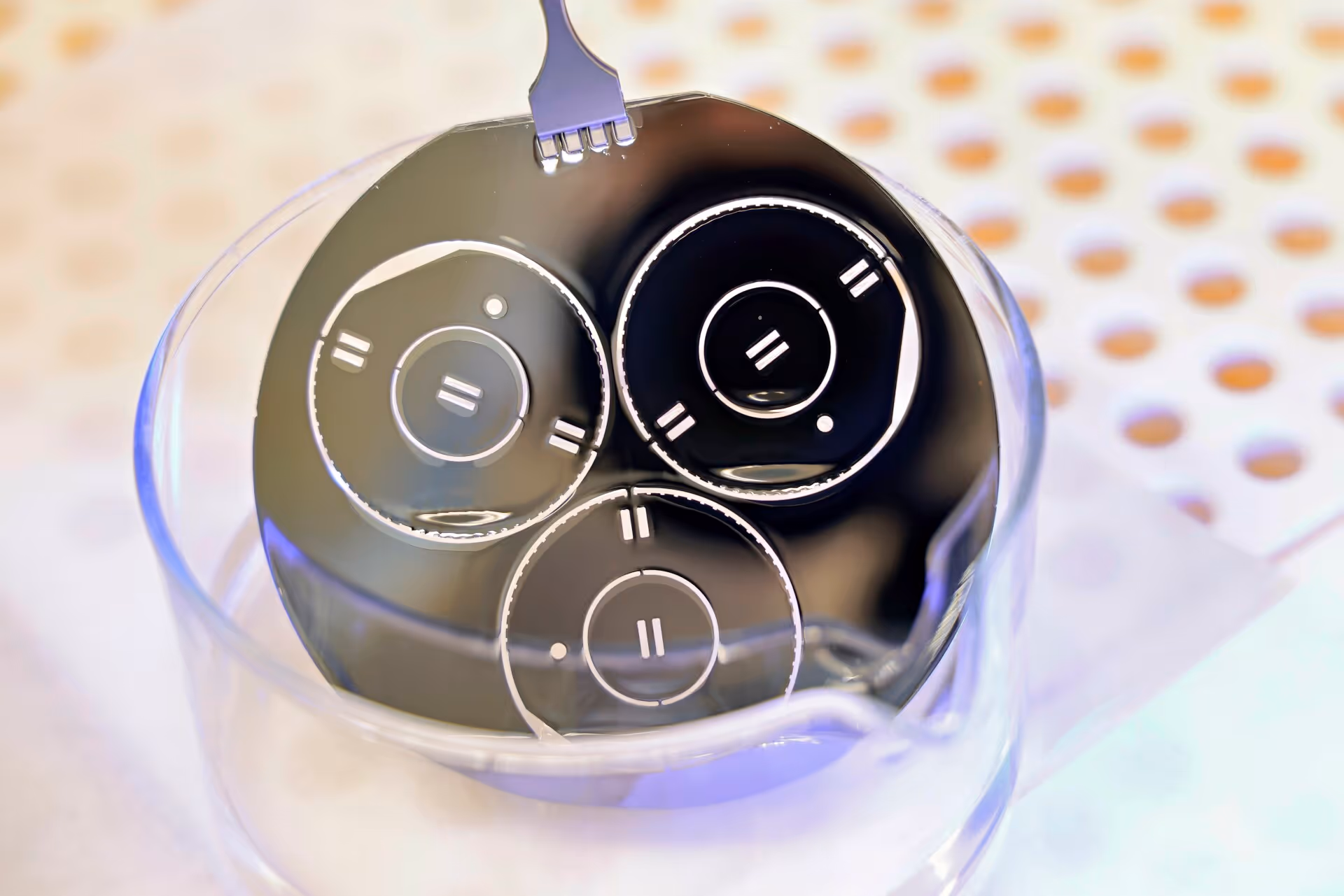
Fabrication
State-of-the-art 4" wafer processing in an ISO 5 cleanroom, with flows tailored for research, prototyping, and pilot production.
Material Selection
High-quality nanomaterial growth with automated characterization and customized selection to match your specifications and ensure consistent performance.
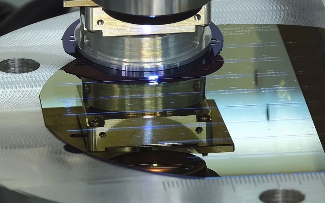
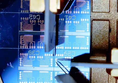
Transfer
Carbon nanotubes transfer with our own equipment system offering high-precision, high-throughput wafer scale integration at room temperature.
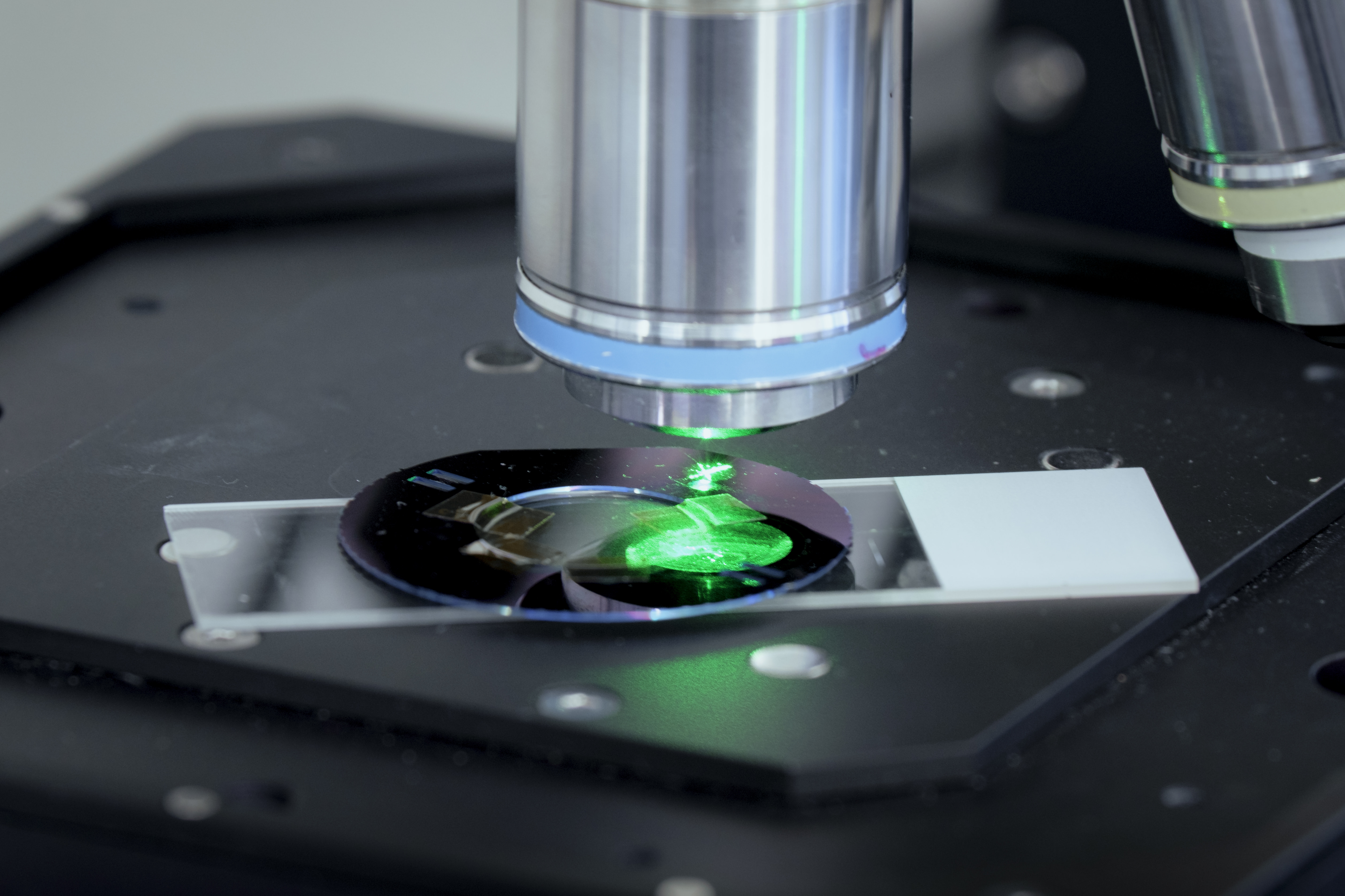
Device Testing
Electrical testing from room temperature down to 4 Kelvin, complemented by optical measurements and SEM imaging to verify alignment, stability, and device performance.
Delivering high-quality customized nanodevices

Clean, contamination-free integration
Our transfer process preserves the pristine properties of carbon nanotubes by avoiding chemicals, high temperatures, and process-induced damage, ensuring optimal device performance.

High-precision and scalable
High precision-automated positioning delivering consistent carbon nanotubes placement across wafers. The industrial-grade automation and cleanroom-compatible processes ensure smooth transition from laboratory research to pilot production and wafer-scale manufacturing.

Tailored device performance
Our machine-learning-based material characterization process allows customized performance selection with high repeatability. A 3-step workflow shortens R&D timelines and allows faster iterations from prototype to qualified device.