Why nanomaterial integration matters
Modern semiconductor scaling is reaching physical limits. To continue improving performance and efficiency, next-generation chips will need to integrate nanomaterials that offer superior electronic and thermal properties to silicon.
Nanomaterials enabling post-silicon electronics
1D nanomaterials
One-dimensional nanomaterials, such as carbon nanotubes and nanowires, are tiny, linear structures with exceptional electrical and thermal conductivity. Their geometry makes them ideal for high-performance transistors, interconnects, and nanoscale sensors, enabling devices that are faster, smaller, and more energy-efficient.
2D nanomaterials
Two-dimensional nanomaterials, like TMDs, hBN and graphene, are atomically thin layers with unique electronic and mechanical properties. Their tunable bandgaps and flexibility allow integration into ultra-thin transistors, flexible electronics, and advanced optoelectronic devices, opening possibilities beyond conventional silicon technology.

How Chiral integrates nanomaterials at wafer scale
Device design
Our team supports you with layout designs and process flow. We can make the full design for you or adapt your design to our process to make it compatible.

Substrate fabrication
We also propose a fabrication service for the receiving wafers if your team does not have access to the relevant facilities.
Nanomaterial growth
Growth of high-quality nanomaterials is the first critical step in our production cycle. We grow high-quality nanomaterials that will be integrated into your devices later.

Nanomaterial characterization
Chiral characterizes its nanomaterials through tailored characterization procedures to ensure their quality and select the materials that are most suitable for your target application.

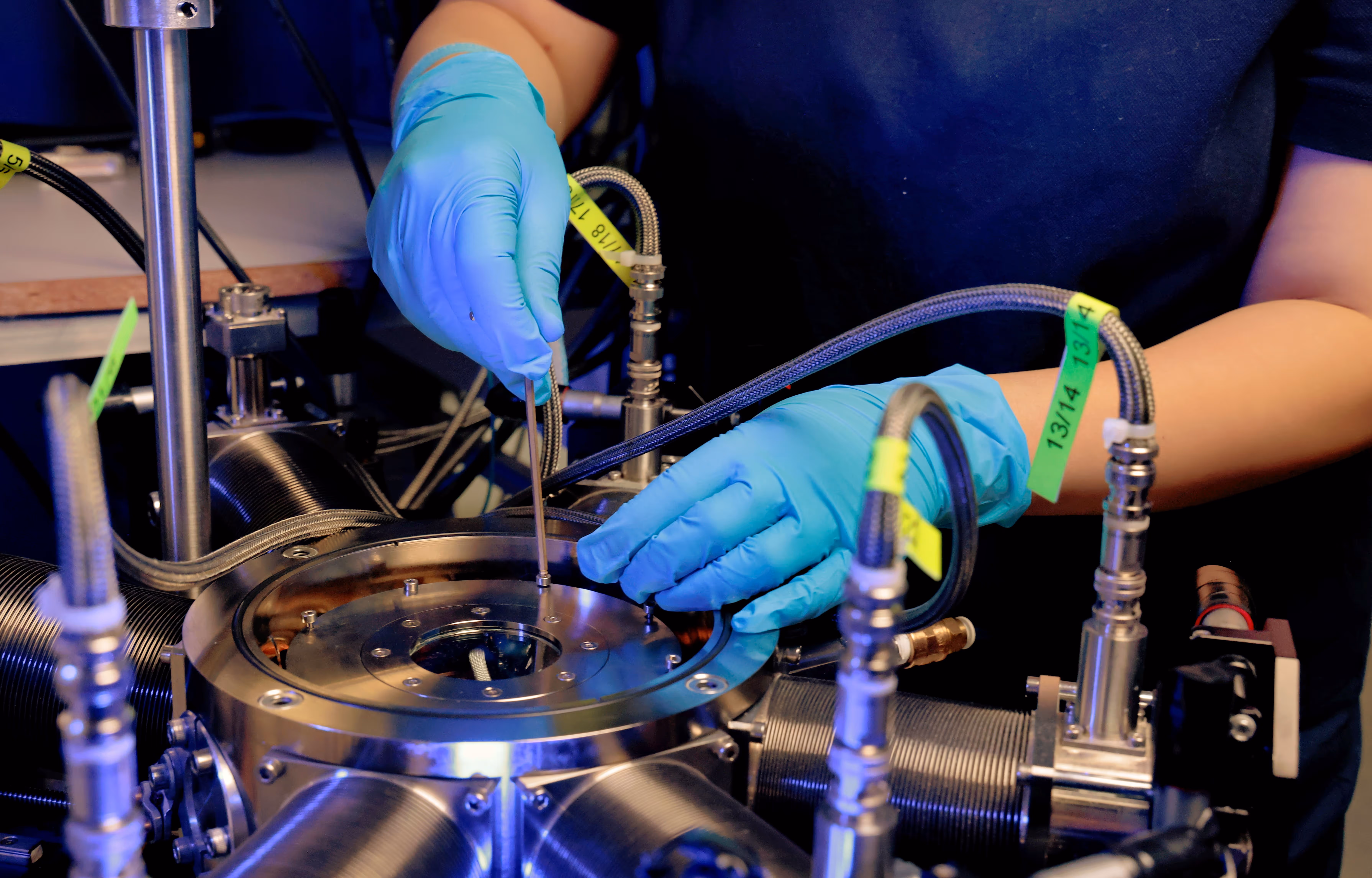
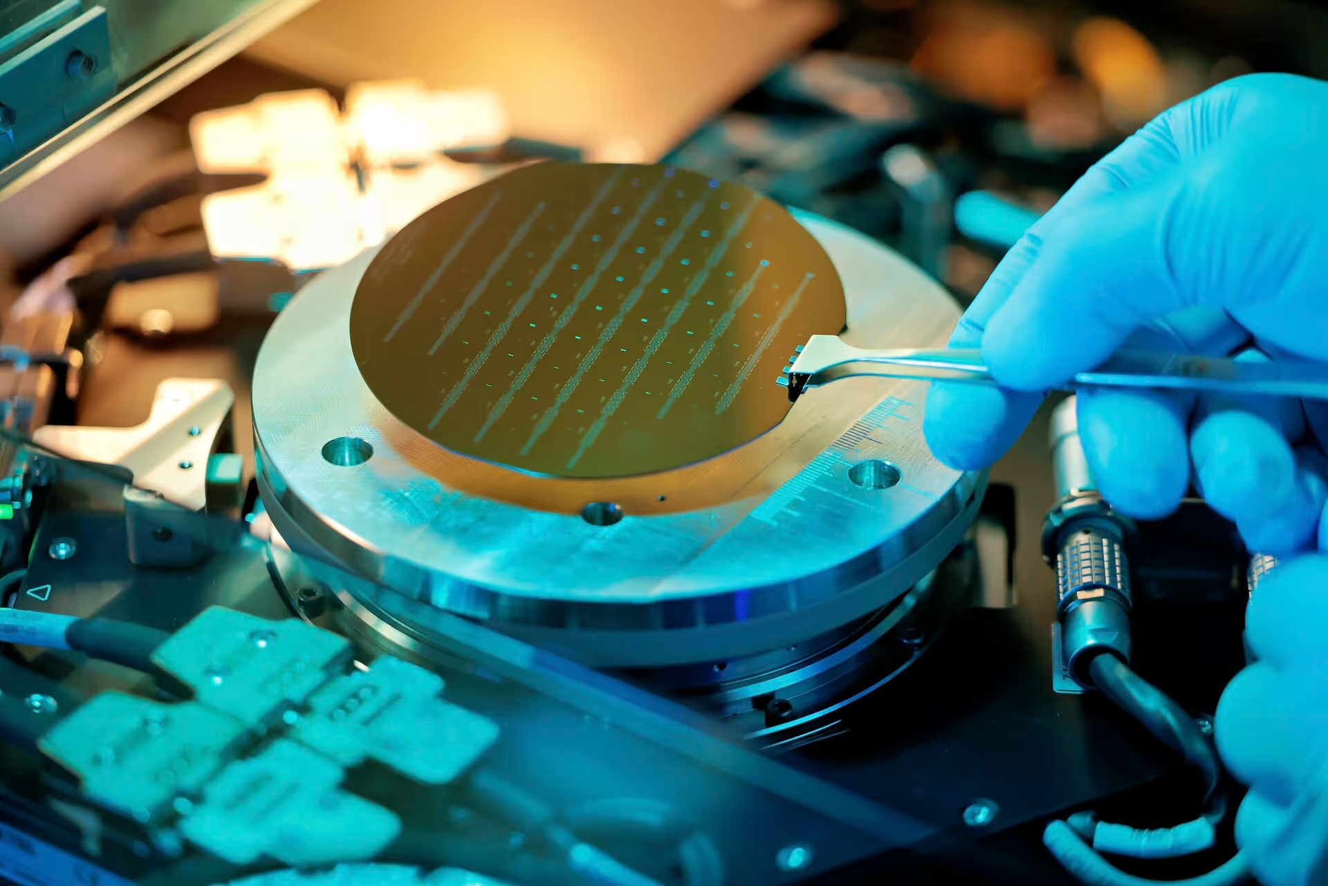
Automated assembly
Our nanoassembly equipment places the selected nanomaterials on target structures. This fully automated machine allows uninterrupted assembly of devices at wafer level with unprecedented precision and speed.

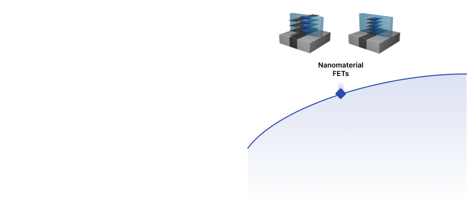
Performance result of the transistor by using nanomaterials